The Kirin 9000S processor in the Huawei Mate 60 Pro has brought the public’s attention to domestic chip manufacturing.
Various clues, such as data read by benchmarking software and third-party teardown reports, indicate that the Kirin 9000S is a 7nm process chip, and its origin is clearly marked as mainland China. However, the EUV, which is specifically used for producing 7nm chips, was already under export control to China in 2019. China’s chip foundries could only obtain DUV lithography machines with a 193nm light source, and this export control is still tightening. Recently, Dutch lithography machine manufacturer ASML confirmed that it will not be able to deliver DUV lithography machines to Chinese customers by 2024.
The question is, how was this 7nm chip produced? The emergence of the 7nm process Kirin 9000S has two main possibilities: one is a breakthrough in domestic EUV lithography machines, and the other is that chip manufacturers have adopted special “magic” on DUV to indirectly produce 7nm process chips.
From an objective perspective, the latter speculation is far more likely than the former, as I also mentioned in the article “China’s Chips, Just Lacking Lithography Machines?” We are not just lacking lithography machines, but also the supporting facilities and breakthroughs in basic research. Even if EUV lithography machines are developed, it will take a year or two to complete the process of large-scale production for commercial chips.
Therefore, in this article, we will focus on explaining why DUV lithography machines used to produce 28nm chips can produce 7nm chips? And we will also talk about why the naming of these process nodes like 7nm and 28nm is a word game. To help everyone understand, we will first lay the groundwork with some knowledge points related to chip manufacturing, including the principle of lithography and the lithography process.
01 Re-understanding Lithography
Using a 193nm DUV (Deep Ultraviolet) lithography machine covers 28nm and above process nodes. Using DUV to manufacture 7nm process chips sounds like an impossible task because the shortest wavelength of the light source of commercial DUV lithography machines is 193nm, which is 28 times the difference from 7nm, seemingly impossible to break through, but the industry has indeed used DUV to manufacture 7nm chips. How is this achieved?
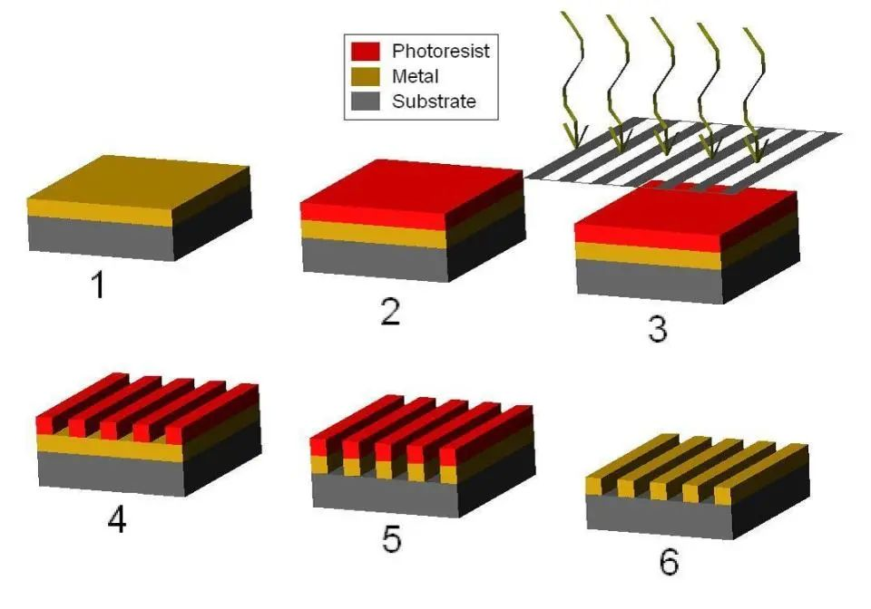
The basic principle of lithography, red is photoresist, yellow is metal layer, gray is wafer (substrate), the top of Figure 3 is the mask plate
First, briefly introduce the principle of the lithography machine and the lithography process of chip production. The principle of lithography is similar to the traditional film movie projection. Projecting a movie is to transmit the pattern from the movie film to the screen, while lithography is to transmit the pattern from the mask plate to the wafer surface, thereby processing specific patterns and lines on the wafer surface (as shown in the figure above).
Specifically, first, the mask plate required for lithography is made, which is equivalent to the film. This requires etching the chip layout with chromium metal onto a special glass to make the mask plate. Then, ultraviolet light is used to pass through the mask plate and irradiate the wafer below.
The pattern on the mask plate (that is, the chromium-plated part) blocks a part of the light, while the pattern that is not blocked can transmit the light, so the circuit pattern is transferred to the wafer surface. The wafer surface is pre-coated with photoresist, and the photoresist that is irradiated undergoes a chemical reaction and is corroded and washed away by a chemical solution, exposing the wafer below, which can be etched by subsequent processes, thereby processing the corresponding patterns and lines on the wafer.
In this way, transistors, metal interconnects, and other chip structures can be processed layer by layer.
In order to process smaller-sized transistors, it is necessary to shorten the wavelength of ultraviolet light, so that the lines processed on the photoresist will be more refined.
The wavelength of the early ultraviolet light was 436nm g-line, which could process transistors with a process size of 500nm or more. As the transistor size continued to shrink, the wavelength of the ultraviolet light source on the lithography machine was shortened to 405nm g-line and 365nm i-line. When the transistor process size was reduced to below 250nm, the corresponding wavelength of the ultraviolet light source needed to be shortened to 248nm and 193nm, which is the range of deep ultraviolet light (DUV).
02 The Word Game of “7nm”
Secondly, I want to emphasize to everyone that the concept of chip manufacturers’ process nodes, such as 7nm, 14nm, 28nm, etc., is a name or specification used by wafer manufacturers to identify chip processing technology.
In the mid-to-late 1990s, the process node was the minimum length (line width) of the transistor gate that the chip factory could achieve, referred to as gate length. However, the current 7nm process node is not truly equal to 7nm in mathematics. Each transistor size on a 7nm process chip is much larger than 7nm, “7nm” is just a “label”.
The reason why 7nm has become a label is inseparable from the naming standards established by semiconductor manufacturers since the 1990s.
According to Moore’s Law and Dennard scaling, the gate length of each generation is reduced to 70% of the previous generation. If the gate length of the previous generation transistor is 1 micrometer, then the next generation is 0.7 micrometers, so the area of each transistor is just halved, or the number of components is doubled.
By 2005, semiconductor manufacturers found that the gate length could not continue to shrink at a rate of 70% per generation, because the shorter the gate length, the greater the leakage current, and the more serious the chip overheating problem. However, the industry has been accustomed to multiplying by 0.7 for each upgrade, so semiconductor manufacturers, regardless of whether the gate length of the next generation can be reduced to 70%, directly multiply the previous generation process node by 0.7 as the new process node, so we have process node names such as 32nm, 22nm, 14nm, 10nm, and 7nm.
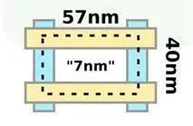
TSMC’s 7nm process: CPP=57nm, MMP=40nm
Since the process node cannot truly reflect the transistor size, what size does the industry use to represent the transistor size? In fact, the industry will use the process gate pitch (CPP) and metal pitch (MMP) to represent it with two sizes (as shown in the figure above), which are equivalent to the length and width of a rectangle, and their product determines the area of the transistor. For example, TSMC’s 7nm process gate pitch (CPP) is equal to 57nm, and the metal pitch (MMP) is 40nm. Samsung is also similar, with these two data being 54nm and 36nm, both of which are far greater than the 7nm claimed by semiconductor manufacturers.
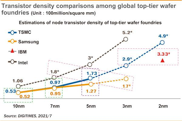
The transistor density corresponding to major chip manufacturers at different nodes, Intel, TSMC, and Samsung’s 10nm nodes, correspond to the number of transistors per square millimeter, which are 1.06 million, 530,000, and 520,000, respectively.
In the past, Intel was more practical and used channel length (smaller than gate length) to define nodes, and there is a saying that it is to closely follow Moore’s Law. Regardless of the reason, the naming is always at a disadvantage compared to its competitors.
For example, Intel’s 10nm has a higher transistor density than TSMC and Samsung’s 7nm (as shown in the figure above), but from a marketing perspective, everyone else says 7nm, and Intel says it is 10nm, which is a disadvantage of being “uneducated”, so later Intel also followed its competitors and changed to node naming methods such as intel 4 and intel 3.
The above explanations are just to tell you that the naming of nodes is a word game, and the minimum metal pitch corresponding to the 7nm process is around 36nm-40nm.
With this understanding, we can talk about the relationship between the 193nm DUV lithography machine mentioned earlier and the 7nm chip to be manufactured. Or to put it this way, DUV production of 7nm chips is actually using a 193nm light source lithography machine to produce chips with a metal pitch of 36nm-40nm.
The 193nm light source and the 36nm metal pitch are about 5 times apart. How to bridge this gap? Here, we have to mention the iteration from DUV dry lithography machines to DUV immersion lithography machines.
Although the wavelength of the light source of the DUV lithography machine is 193nm, the light will refract in water, and the wavelength will be shortened. The refractive index of 193nm ultraviolet light in water is 1.44, and the wavelength is 134nm. Based on this principle, Lin Benjian proposed immersion lithography in 1987, which is to add a layer of ultra-pure water between the wafer surface and the lens to refract the ultraviolet light, thereby reducing the wavelength to 134nm. In 2003, ASML of the Netherlands implemented the immersion lithography machine for the first time based on this research.
From DUV dry lithography machines to DUV immersion lithography machines, from a 193nm light source wavelength to a 134nm wavelength of ultraviolet light, this gap with the 36nm metal pitch is further reduced to 4 times.
03 Multiple Exposure to Complete the “Last Kilometer”
The emergence of immersion lithography machines has once again narrowed the gap with the “7nm” process, but the industry still cannot directly use this kind of lithography machine to process the “7nm” chips that everyone is talking about. If chip manufacturers really want to manufacture the rumored 7nm Kirin 9000S, double exposure and multiple exposure are essential.
To explain the double exposure technology, let’s take a photography example. Suppose you are a photographer and you want to take a picture of a sports meeting queue. This queue has only 20 people, and they stand apart at a distance of 2 meters, which looks very sparse. How do you take a picture of 40 people? You have a solution: first take the first picture, and then let each person move 1 meter, take another picture, and then combine the two pictures through software.
Double exposure technology can also be used in the same way. Use a set of mask plates to process lines with a spacing of 134nm, and then use another set of mask plates to translate a certain distance to process another set of lines with a spacing of 134nm. When the two are combined, there are lines with a spacing of 67nm, which is another step forward from 36nm. From 22/20nm, the industry began to introduce double exposure technology.
In order to achieve double exposure technology, the industry has developed the LELE method (lithography-etching-lithography-etching), which requires two coatings of photoresist and two exposures. The first exposure copies the pattern on the hard mask, and the second exposure copies the minimum line width pattern on the photoresist. However, due to the use of two exposure equipment, the manufacturing cost has greatly increased, and the time spent is also longer. You know that lithography accounts for about 50% of the entire manufacturing time, and doubling the exposure will greatly extend the entire manufacturing time.
To this end, the industry has also developed a more efficient self-aligned double patterning method (SAPD). This method reduces the two coatings of photoresist to one, and it uses chemical vapor deposition (CVD) technology to deposit silicon oxide around the first coated photoresist, naturally forming an aligned processing position, so that the second graphic processing can be achieved.
With these technologies, double exposure can process a metal pitch of 67nm, but this is still twice as far from 36nm. How to break through the last two times the gap?
There is a simple and crude method, which is to do another double exposure, a total of four exposures, and then halve the 67nm again, processing the minimum line width of 34nm, which just meets the 36nm metal pitch required for processing 7nm.
However, the price to be paid for this method is really too high. The exposure time is 4 times that of single exposure, and more mask plates need to be prepared. Each exposure requires more supporting processes (photoresist coating, soft baking, alignment, development, spin drying, hard baking, graphic inspection, etc.), and the total manufacturing processes required increase from hundreds to thousands, which greatly increases the time cost and material cost of manufacturing. In addition, the increase in exposure time will increase the heat of the lens, and the increase in temperature will also lead to the deformation of the lens optical path, and the overlay accuracy is more difficult to control. The difficulty of matching thin films and etching processes has also greatly increased. In addition, the above calculations do not consider the influence of numerical aperture (NA) on lithography accuracy (this part does not involve the understanding of multiple exposures, so this article does not elaborate on overlay accuracy and numerical aperture). In order to improve the numerical aperture, the lens also needs to be made larger.
Based on multiple exposure technology, TSMC began to use DUV to produce 7nm chips (N7) in June 2016, and Samsung began to mass-produce 7nm chips (7LPP) with DUV in 2018. From then on, using DUV to achieve 7nm process became a reality.
In a nutshell, although it is possible to use multiple exposure methods to use the 193nm light source DUV to produce 7nm chips, the time, material, and labor costs will be greatly increased, and the yield will also be affected due to the extreme increase in processes.
In contrast, EUV has a wavelength of only 13.5nm, and 7nm chips can be made with one exposure, but EUV has whetted the appetite of wafer factories, and it was not officially used on the 5nm process until 2020. Before that, GlobalFoundry lost patience and announced that it would stop the development of 7nm technology due to the high cost.
04 Can DUV Break Through 5nm Process?
However, this is not the whole story.
In addition to multiple exposure technology, using DUV to process 7nm process also requires the cooperation of many technologies to achieve, including phase shift mask (PSM), off-axis illumination, optical proximity correction (OPC), optimized aperture and lithography graphics (SMO), etc. These technologies have given rise to a new sub-discipline: computational lithography. The huge amount of data required by it makes NVIDIA’s GPU chips also become the tools needed for calculation, and it has launched the cuLitho software acceleration library, which claims to speed up the time of computational lithography by 40 times.
The reason why computational lithography is needed is because when the lines on the mask plate become very small, the ultraviolet light will produce deviations when passing through the mask plate, causing the lithography graphics to distort. To this end, researchers came up with a method to pre-calculate the possible distortion on the mask plate, so as to reverse design the optimal shape of the mask plate required for lithography, and offset these distortions in advance, which is called reverse lithography calculation, and this requires a very large amount of calculation, and ordinary computers are simply unable to bear it, so researchers have to use supercomputers and cloud computing.
At the same time, researchers have also applied artificial intelligence’s machine learning algorithms to computational lithography. The new generation of convolutional artificial neural networks is applied to lithography process models, mask optimization, SEM data processing, etc., and the training data also requires a huge GPU chip set. In addition to the optimization of the device level, researchers have even incorporated the factors to be considered in circuit design into device manufacturing, and considered the impact on manufacturing and lithography in the circuit design stage, which is called DTCO (design and process technology co-optimization), and this requires EDA vendors to upgrade algorithms and software.
It can be said that in order to enable DUV to manufacture 7nm process chips, the industry has done everything possible. If DUV is used to manufacture 5nm process chips next, four exposures are not enough, and 6-8 exposures are needed, as well as more mask plates, longer lithography time, and higher material costs, which has become an unbearable burden. Therefore, when the 5nm chip came out, the EUV lithography machine was also ready, which freed the industry from the cumbersome multiple exposures, and the 7nm process also became the last generation of process manufactured by DUV in the industry.
About the author:
“A Brief History of Chips” Author: Wang Bo, published in 2023, *Dr. Wang Bo, the author, is a chip research expert and a science popularization writer. He has more than 20 years of research and teaching experience at Huawei, the French Lyon Nanotechnology National Laboratory, and the Shenzhen Graduate School of Peking University. He has written “A Brief History of Chips”, “The Question of Time”, and “The Question of Time · Youth Edition”, among which “A Brief History of Chips” was selected as one of the top ten books of the “South China Book Fair” in 2023, a good book on the lighthouse, the third phase of the “New Discovery · Science Popularization Book List”, the top 10 influential books in the first half of 2023 by Baidao.com, and the second quarter 2023 influential book list of China Media Publishing Business Daily.
Discover more from 自由档案馆
Subscribe to get the latest posts sent to your email.